Skip to content
There are two basic kinds of circuit boards:
- Single-layer PCBs have one layer of copper (conductive material) on a base.
- Double-layer PCBs have two layers of copper on a base.
When you need more space for wires or better signal quality, multi-layer PCBs are the better choice.
Unlike single or double-layer boards, multi-layer PCBs are built by stacking many alternating layers of copper and insulation together. This creates a complex wiring network inside the board.
This stack of layers usually includes:
- Copper layers (for the wires/circuits)
- Cores (stiff insulating sheets)
- Base materials (substrates)
- Prepreg (a sticky, glue-like insulating material)
Both prepreg and core are types of insulating material used inside PCBs.
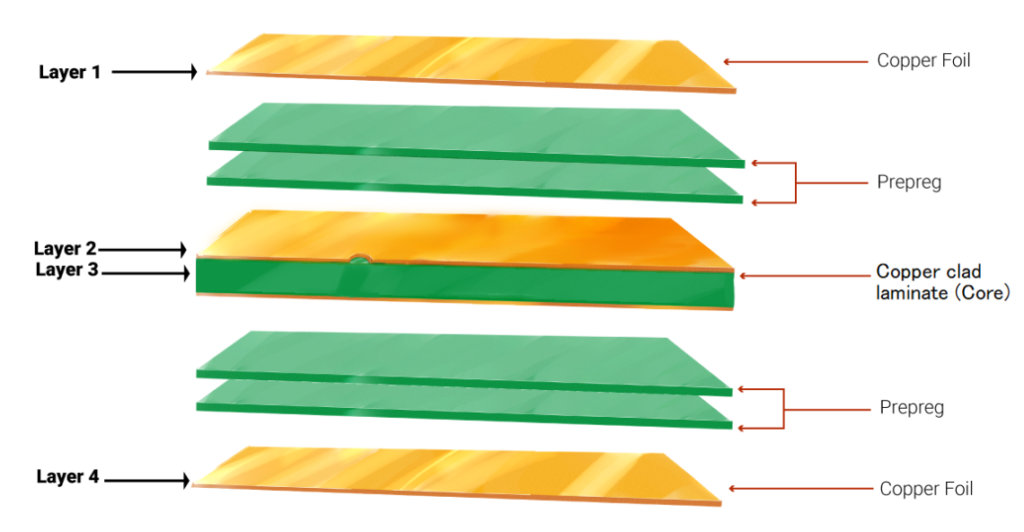
What is prepreg in PCBs?
Prepreg (short for “pre-impregnated”) is a fiberglass layer soaked in sticky, uncured epoxy glue. Unlike other PCB materials, it doesn’t have copper foil attached.
In PCB layer stacks, prepreg does two important jobs:
- It insulates layers from each other
- It acts like glue to hold layers together
During assembly:
- Prepreg is sandwiched between copper layers
- Or placed between copper and core (the stiff base layer)
When heated and pressed during manufacturing:
The sticky epoxy melts and flows, then hardens permanently, bonding all layers into one solid board.
How HDI Circuit Boards Are Layered
Traditional vs. HDI Boards:
Regular PCBs use through-hole vias (drilled through all layers) to connect circuits.
HDI boards use special small vias:
- Micro-vias (tiny laser-drilled holes)
- Blind vias (connect surface to inner layer)
- Buried vias (connect inner layers only)
→ This allows more wiring in less space and better signal quality.
Understanding X-N-X Structure:
This naming pattern describes HDI layer arrangements:
- X = Number of HDI layers (with micro-vias)
- N = Number of standard core layers between them
Common patterns:
1-N-1 • 2-N-2 • 3-N-3
Example: 1-4-1 Stack-up
Imagine the PCB from top to bottom:
1️⃣ Top layer: HDI (with micro-vias)
⬇️
2️⃣-5️⃣ Four core layers (standard connections)
⬇️
6️⃣ Bottom layer: HDI (with micro-vias)
(Like a sandwich: HDI bread → core filling → HDI bread)