Skip to content
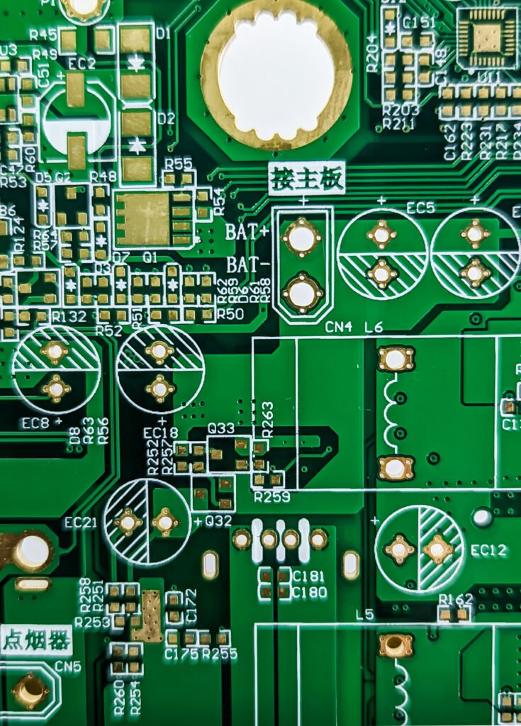
PCB silkscreen printing is a process used to apply printed text, symbols, marks, and images to the surface of a printed circuit board (PCB). This layer, referred to as the silkscreen, is an integral part of the PCB manufacturing process. It involves applying a specialized ink or ink-like substance onto the PCB surface to provide information such as component placement, assembly instructions, and identification markings.
The silkscreen layer is typically printed on the top side of the PCB, also known as the component side. This layer can include a variety of details, such as warning symbols, assembly guidelines, component names, brand logos, and other indicators. It is applied after completing the solder mask and circuit layers, serving as a crucial aid for assembly and maintenance.
During the silkscreen process, ink is applied to the PCB using a fine mesh screen or stencil, with contrasting colors like white or black to ensure readability against the PCB’s background. This step occurs late in the PCB production process, helping ensure accurate and detailed markings.
If you want to know more about Silkscreen Printing, please visit my post about “How to Design Character Parameters on PCB Board?”
What Advantages of PCB Silkscreen Printing?
Silkscreen printing on PCBs offers numerous benefits:
- Component Identification: Helps quickly identify components during assembly and troubleshooting.
- Assembly Guidance: Provides clear instructions for efficient PCB assembly.
- Circuit Understanding: Simplifies interpreting the board’s design.
- Branding and Logos: Allows manufacturers to add logos or branding for easy identification.
- Aesthetics: Enhances the overall look of the board.
- Compliance and Certification: Marks essential certification and regulatory information.
- Documentation and Reference: Offers permanent reference details on the PCB itself.
For example, silkscreen markings can label different components, making them easier to identify during testing, assembly, or repairs. For multilayer PCBs, silkscreen printing can also indicate the number of layers, helping ensure correct stacking during manufacturing.
The Methods of Creating PCB Silkscreen?
There are three main methods used for creating PCB silkscreen layers, each with its advantages and disadvantages:
1. Manual Screen Printing
This traditional method involves manually applying ink to the PCB using a nylon tracing stencil. The stencil aligns with the PCB design, and the ink is applied, followed by curing in an oven to solidify the markings. This method is suitable when line widths are above 7 mm and registration tolerances are around 5 mm.
Pros:
- Cost-Effective for Small-Scale Production: Ideal for limited runs with minimal setup and equipment costs.
- Versatility: Can print on various materials and both flat and curved surfaces.
- Flexible Design Modifications: Allows on-the-fly adjustments for small batch production.
Cons:
- Labor-Intensive: Requires skilled operators to ensure precision and consistency.
- Low Resolution: Not ideal for intricate designs or fine details compared to automated methods.
- Limited Efficiency: Unsuitable for large-scale production due to slower processing speeds.
2. Liquid Photo Imaging (LPI)
Liquid photo imaging involves coating the PCB surface with liquid epoxy that reacts to UV light. The silkscreen design is transferred onto the PCB using UV exposure, followed by a development process. LPI is commonly used for solder mask applications as well as silkscreen printing.
Pros:
- Versatility: Suitable for multiple PCB applications, including solder masks and silkscreen layers.
- High Resolution: Produces intricate patterns and fine details with precise layer alignment.
- Accuracy: Digital files and UV exposure ensure consistent results.
Cons:
- Time-Consuming: Exposure and development steps can be lengthy, particularly for complex designs or large-scale production.
- Complex Process: Requires careful control of variables such as exposure time and drying conditions to maintain consistency.
3. Direct Legend Printing (DLP)
DLP is a digital printing method that uses a projector or light source to selectively cure liquid resin layer by layer. This modern approach is highly precise and increasingly popular in PCB manufacturing.
Pros:
- High Precision and Resolution: Ideal for intricate designs and accurate registration of fine details.
- Faster Production Times: Simultaneous curing of multiple layers accelerates production cycles.
- Customizable: Digital files allow easy adjustments, making it perfect for prototyping and design iteration.
Cons:
- High Initial Cost: DLP systems require significant investment in equipment and materials.
- Limited Material Selection: Primarily suited for resin-based materials, which may lack the versatility of traditional PCB substrates.
Why Choose Silkscreen Printing for PCBs?
Silkscreen printing remains an essential step in PCB manufacturing due to its practical advantages. It supports component identification, provides assembly guidance, and aids in circuit understanding. Additionally, it allows manufacturers to incorporate branding, logos, and certification marks, contributing to both functionality and aesthetics.
When selecting a silkscreen method, it is important to consider project-specific factors such as production volume, design complexity, budget, and desired print quality. While manual screen printing may suffice for simple designs or low volumes, more complex or high-resolution requirements may benefit from LPI or DLP methods.
Ultimately, PCB silkscreen printing plays a critical role in ensuring the usability, clarity, and professional appearance of printed circuit boards, making it an indispensable part of modern electronics manufacturing.