Skip to content
PCB panelization plays a pivotal role in circuit board design, as its dimensions critically influence production efficiency, assembly workflows, and overall project economics. Serving as the foundational framework for modern electronics – from household appliances to industrial machinery – optimized panel sizing ensures cost-effective manufacturing while meeting application-specific demands. This guide examines four key aspects: 1) Why panel size matters for yield optimization, 2) Key constraints (equipment limits/material yields), 3) Layout strategies to minimize waste, and 4) Industry-specific best practices across consumer, automotive, and aerospace sectors.
What is PCB Panel Size?
Think of PCB panel size like a “baking sheet” for circuit boards. It’s the standard-sized board manufacturers use to mass-produce your individual PCBs.
Key Factors influencing PCB Panel Size?
PCB panel size optimization balances manufacturing capabilities, cost efficiency, and design requirements. Here’s a breakdown of the critical factors:
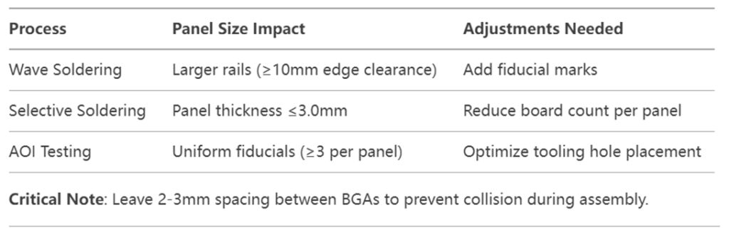
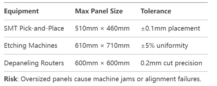
1. Manufacturing Equipment Limits
SMT Pick-and-Place Machines: Max load size (e.g., 510mm×460mm for Fuji NXT III).
Exposure Machines: Lithography area limits (e.g., 610mm×710mm).
CNC/Routing Machines: Worktable dimensions (e.g., 1000mm×1200mm for automotive PCBs).
2 Material Utilization
Standard Raw Panel Sizes: Common PI sheets are 250mm×600mm.
Breakaway Tabs: V-cut requires 3-5mm edges; mouse bites need 8-10mm.
3 Assembly Process Requirements
4 PCB Design Characteristics
Thickness: Thin boards (<0.4mm) need smaller panels to avoid warping.
Layer Count: High-layer boards (≥8L) work best with ≤400×300mm panels.
Flex PCBs: FPCs typically use 250×150mm panels to minimize stretching.
What Challenges in PCB Panel Size?
Designing PCB panels involves balancing technical constraints, cost, and manufacturability. Here are the key challenges and their implications:
1 Material Waste vs. Utilization Efficiency
Challenge: Irregular board shapes or suboptimal layouts lead to wasted raw material.
Consequences: Scrap rates exceeding 15–25% for complex designs.
Higher costs for specialty materials (e.g., high-frequency laminates).
2 Equipment Compatibility
Challenge: Panel sizes must align with factory machinery limits.
3 Mechanical Stress & Warping
Challenge: Large panels are prone to bending during assembly.
4 Cost-Driven Design Pressures
Engineers want larger panels for testing, while procurement pushes for smaller sizes to cut costs.
How to Choose the Right PCB Panel Size?
Selecting the optimal PCB panel size requires balancing design requirements, manufacturing capabilities, and cost efficiency. Here’s a structured approach to ensure success:
1 Start with Application Requirements
Taking into account the final environmental application, such as flexible circuits, the use of small-sized panels is adopted to reduce warpage phenomena.
Taking into account the density of components, for instance, high-density designs (such as BGA type) require that the spacing between boards should be no less than 2 millimeters.
2 Consult Manufacturer Specifications
Confirm with the manufacturers the production capabilities of the core equipments, such as the exposure machine, etching machine or surface mount machine.
3 Balance Cost and Volume
The number of the panels should be as large as possible to make full use of the raw materials and reduce waste.
Strategic PCB panelization is critical for enhancing production line throughput, cost optimization, and maintaining reliability standards. Through systematic analysis of panelization constraints – including material utilization rates, SMT equipment compatibility, and depaneling methodologies – manufacturers can implement data-driven solutions to achieve >92% material yield while mitigating warpage risks.